Nanofabrication/Equipment/Wafer Dicing Saw: Difference between revisions
< Nanofabrication | Equipment
Jump to navigation
Jump to search
(Created page with "<gallery> IMG 0956.JPG |Wafer Mounting System Example.jpg|Caption2 </gallery>") |
|||
| (6 intermediate revisions by the same user not shown) | |||
| Line 1: | Line 1: | ||
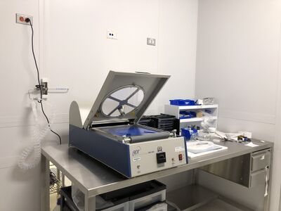
IMG 0956.JPG |Wafer Mounting System | |||
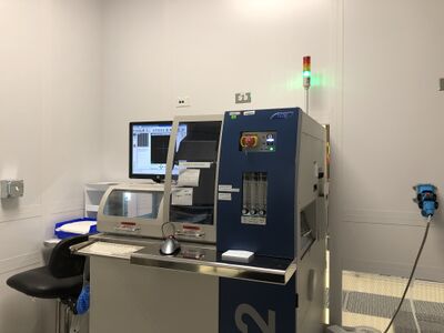
[[File:IMG 0955.JPG|right|400px| ADT 7200 Dicing Saw]] | |||
[[File:IMG 0956.JPG|right|400px|Wafer Mounting System]] | |||
==Dicing Saw== | |||
The ADT7200 Dicing saw is a semiautomatic saw that can cut up from small pieces to a 200mm silicon wafer. | |||
===Features=== | |||
* 8 Inch Chuck | |||
materials cut: Silicon, Glass, Sapphire, Quartz, STO | |||
===Thing to know=== | |||
* Each user should know or do the following before cutting or requesting staff assistance in cutting: | |||
* Substrate thickness and composition. | |||
* Blue dicing tape thickness: 75 microns (other tape may be a different thickness). | |||
* Spin thin photoresist layer to protect surface if needed. | |||
* Index for all angles | |||
* Where markers are located | |||
* No GaAs, PZT, or heavy metals are allowed. | |||
===Dicing Blades=== | |||
===User Proposal Feasibility=== | |||
When requesting the use of this instrument, please provide the following information in your user proposal: | |||
* Sample materials | |||
* Layout Drawing | |||
* Number of samples to process or number of times of instrument usage | |||
Questions? Please contact the instrument custodian before submitting your proposal. | |||
Latest revision as of 00:40, January 29, 2021
Dicing Saw
The ADT7200 Dicing saw is a semiautomatic saw that can cut up from small pieces to a 200mm silicon wafer.
Features
- 8 Inch Chuck
materials cut: Silicon, Glass, Sapphire, Quartz, STO
Thing to know
- Each user should know or do the following before cutting or requesting staff assistance in cutting:
- Substrate thickness and composition.
- Blue dicing tape thickness: 75 microns (other tape may be a different thickness).
- Spin thin photoresist layer to protect surface if needed.
- Index for all angles
- Where markers are located
- No GaAs, PZT, or heavy metals are allowed.
Dicing Blades
User Proposal Feasibility
When requesting the use of this instrument, please provide the following information in your user proposal:
- Sample materials
- Layout Drawing
- Number of samples to process or number of times of instrument usage
Questions? Please contact the instrument custodian before submitting your proposal.

