Nanofabrication/Equipment/Wafer Dicing Saw: Difference between revisions
< Nanofabrication | Equipment
Jump to navigation
Jump to search
No edit summary |
No edit summary |
||
| Line 1: | Line 1: | ||
IMG | |||
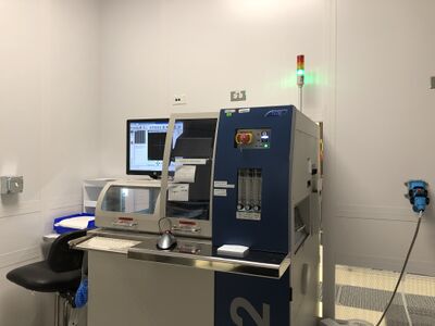
IMG | [[File:IMG 0955.JPG|right|400px| ADT 7200 Dicing Saw]] | ||
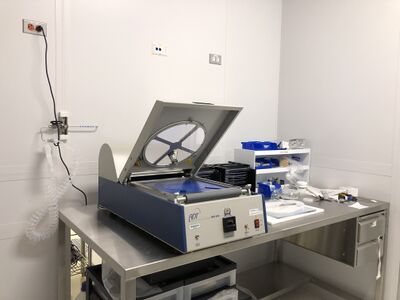
[[File:IMG 0956.JPG|right|400px| ADT 7200 Dicing Saw]] | |||
==Dicing Saw== | |||
===Features=== | |||
* 8 Inch Chuck | |||
materials cut: Silicon, Glass, Sapphire, Quartz, STO | |||
===User Proposal Feasibility=== | |||
When requesting the use of this instrument, please provide the following information in your user proposal: | |||
* Sample materials, shapes, and sizes | |||
* Information about the intended patterns (shapes, sizes, distances, area coverage) | |||
* Number of samples to process or number of times of instrument usage | |||
Questions? Please contact the instrument custodian before submitting your proposal. | |||
Revision as of 20:02, November 23, 2020
Dicing Saw
Features
- 8 Inch Chuck
materials cut: Silicon, Glass, Sapphire, Quartz, STO
User Proposal Feasibility
When requesting the use of this instrument, please provide the following information in your user proposal:
- Sample materials, shapes, and sizes
- Information about the intended patterns (shapes, sizes, distances, area coverage)
- Number of samples to process or number of times of instrument usage
Questions? Please contact the instrument custodian before submitting your proposal.

