ANL Digitizer Firmware for Advanced Users: Difference between revisions
No edit summary |
|||
| Line 25: | Line 25: | ||
The digitizer can run standalone without being connected to a trigger system. In this configuration every digitizer board has independent and unsynchronized clocks. Timestamps for event sorting are not useful across multiple modules as there is no synchronism, but within one board timestamps are still sensible. | The digitizer can run standalone without being connected to a trigger system. In this configuration every digitizer board has independent and unsynchronized clocks. Timestamps for event sorting are not useful across multiple modules as there is no synchronism, but within one board timestamps are still sensible. | ||
''See [[ | ''See [[MyRIAD_USER_Manaual]] or [[MyRIAD_Abridged_User_Notes]] for detailed information on External Trigger systems''. | ||
== General Design of the Firmware == | == General Design of the Firmware == | ||
Revision as of 20:49, September 27, 2021
A Short Introduction to Hardware
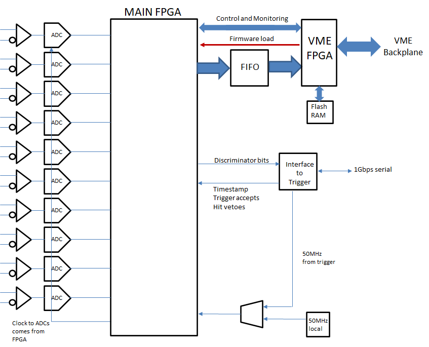
To fully understand how the firmware works the hardware environment must be explained. The digitizer module contains two FPGAs, one for VME interface and firmware maintenance purposes, and the other for ADC data processing, as shown in Figure 1.

Input Signals
Signals at the digitizer input are differential. The input range is limited. While the ADC chip the module uses nominally has a +/-2V differential input (that is, + to – may range from -2V to +2V) the input buffer circuitry does not have sufficient power supply voltage headroom to support this full range. The device works very well for signals that range between -1.5V to +1.5V differential, but signal compression occurs beyond those limits. Linearity studies performed at ANL show that the device is almost perfectly linear for an input range of -1.2V to +1.2V but small deviations from linearity are discernable from 1.2V to 1.5V with marked deviations occurring past 1.5V.
In terms of ADC counts, since the ADC chip is designed to span 16,384 codes over 4 volts, this means that the conversion is 4096 counts per volt. Thus
- For absolute best linearity, limit the DC offset and signal range to no more than ±(1.2 * 4096), or ±4916 counts, from the nominal 0V level of 8192 counts (3276 to 13108).
- For all but the most stringent requirements, a more relaxed range of ±(1.5 * 4096), or ±6144 counts, will suffice (2048 to 14336).
- If the physical setup exceeds these bounds, non-linearity will distort waveform shapes.
"Master" and "Slave" Digitizers
The digitizer modules may be used in pairs where one digitizer is labeled the “master” and the other is labeled the “slave”. In this configuration the two digitizers have different versions of firmware. The “master” digitizer alone connects to the trigger system. A ribbon cable connects the “master” digitizer to the “slave” digitizer. The “slave” digitizer channels are normally configured to use signals from the “master” digitizer as part of the logic determining if discriminators within the “slave” channels will fire or not, or whether events within the “slave” are marked for readout or not.
Clocking and Timestamps
The ADC chips run at a frequency of 100MHz (100 MSamp/sec). The device may run from its own internal oscillator or may receive a clock from an external trigger system and synchronize to that clock. A clock distribution from the trigger allows many digitizer modules to run synchronous to each other.
The digitizer module uses a 48-bit timestamp counter run from the 100MHz clock. When connected to the trigger system, the trigger may issue a command to synchronously reset the timestamp in all digitizers. Events read out of the digitizer are tagged with a timestamp for sorting and analysis.
Connection to External Trigger System
Digitizer modules may connect to a trigger system for synchronization and event selection purposes. A separate cable plant connects digitizer modules to trigger modules; on the digitizer end the cable uses the same RJ45 connector as Ethernet, but the signal levels and usage are not Ethernet. Do not connect the digitizer to an Ethernet port, this will damage the digitizer module.
The digitizer can run standalone without being connected to a trigger system. In this configuration every digitizer board has independent and unsynchronized clocks. Timestamps for event sorting are not useful across multiple modules as there is no synchronism, but within one board timestamps are still sensible.
See MyRIAD_USER_Manaual or MyRIAD_Abridged_User_Notes for detailed information on External Trigger systems.
General Design of the Firmware
The ANL version of digitizer firmware implements ten independent data acquisition pipelines in ten channels. Pileup detection & rejection is performed locally within the digitizer. Selective readout of events is achieved using an external trigger system. Waveform readout of all events is possible, with up to 1024 ADC samples per channel per event, although this will limit the event rate as the VME backplane reaches its bandwidth limit. A down-sampling mode allows readout of averaged samples where each waveform sample in the readout may be the average of 2n ADC samples, from 2 to 128 (n = 0, 1, 2,…, 6, 7). Increased event rates are obtained by limiting the amount of waveform data read out per event.
Each channel pipeline consists of a series of memory buffers used for delay. Discriminator logic recognizes edges within the input signal and causes data values to be sampled. When sampling occurs, the timestamp value is saved. The discriminator logic may be configured as either leading-edge (slope) or constant-fraction architecture, sensitive to either positive-only, negative-only or both edges. The discriminator implements a programmable hold-off time to ensure that the discriminator fires only once per edge. A discriminator firing captures timing and data sums simultaneously. This data is buffered so that discriminator re-arms very quickly. Firing rates over 1MHz can be supported, yet readout is limited to the IOCs total bandwidth (IOC Code Design). No information reduction occurs in pileup conditions due to the fast discriminator recovery time.