ANL Digitizer Firmware for Advanced Users
A Short Introduction to Data Acquisition Hardware
To fully understand how the firmware works the hardware environment must be explained. This section briefly introduces the concept of Master and Slave digitizers, Clocking and Timestamps, and Connecting the Trigger to External Systems.
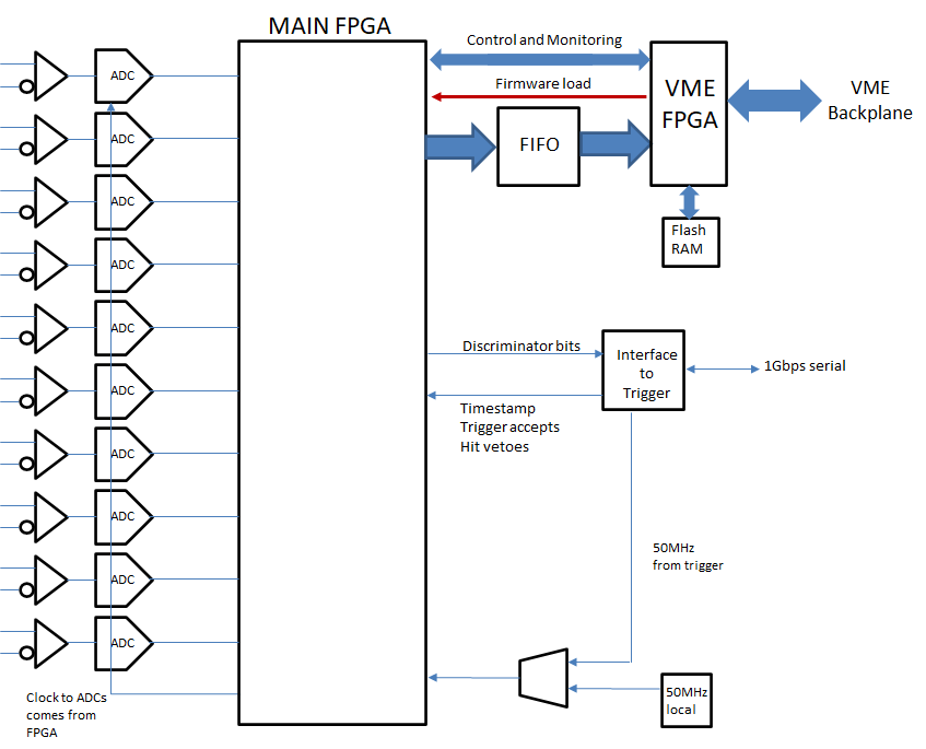
The digitizer module contains two FPGAs, one for VME interface and firmware maintenance purposes, and the other for ADC data processing, as shown in Figure 1.
Input Signals
Signals at the digitizer input are differential. The input range is limited. While the ADC chip the module uses nominally has a +/-2V differential input (that is, + to – may range from -2V to +2V) the input buffer circuitry does not have sufficient power supply voltage headroom to support this full range. The device works very well for signals that range between -1.5V to +1.5V differential, but signal compression occurs beyond those limits. Linearity studies performed at ANL show that the device is almost perfectly linear for an input range of -1.2V to +1.2V but small deviations from linearity are discernable from 1.2V to 1.5V with marked deviations occurring past 1.5V.
In terms of ADC counts, since the ADC chip is designed to span 16,384 codes over 4 volts, this means that the conversion is 4096 counts per volt. Thus
- For absolute best linearity, limit the DC offset and signal range to no more than ±(1.2 * 4096), or ±4916 counts, from the nominal 0V level of 8192 counts (3276 to 13108).
- For all but the most stringent requirements, a more relaxed range of ±(1.5 * 4096), or ±6144 counts, will suffice (2048 to 14336).
- If the physical setup exceeds these bounds, non-linearity will distort waveform shapes.
General Design of the Firmware
This section introduces mid-level descriptions for the topics of Event Data Nomenclature, Discriminator Modes, Pileup Rejection, and Diagnostic Counters.
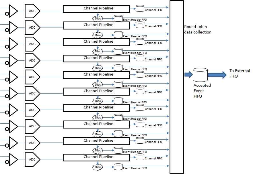
The ANL version of digitizer firmware implements ten independent data acquisition pipelines in ten channels. Pileup detection & rejection is performed locally within the digitizer. Waveform readout of all events is possible, with up to 1024 ADC samples per channel per event, although this will limit the event rate as the VME backplane reaches its bandwidth limit.
Each channel pipeline consists of a series of memory buffers used for delay. When sampling occurs, the timestamp value is saved. The discriminator logic may be configured as either leading-edge (slope) or constant-fraction architecture, sensitive to either positive-only, negative-only or both edges. Firing rates over 1MHz can be supported, yet readout is limited to the IOCs total bandwidth (IOC Code Design).
All sampled values and sums are formatted into an event header that is followed by a programmable number of waveform samples. The header contains various fields, including the timestamp of the event, the timestamp of the last time the discriminator of that channel fired, the timestamp of the peak, energy information, plus some energy/time information carried over from the previous discriminator firing.
Energy measurement is performed in a double-correlated method timed relative to the moment the discriminator fires. Programmable delay buffers positioned to measure ranges of time before (pre-rise) and after (post-rise) the discriminator logic have accumulators continuously calculating the sum of all the ADC samples within them. These sums may then be used by open source user-maintained software (see the gitlab link in analysis codes for GEBSort) to calculate the energy (amplitude) of the input signal, with all necessary baseline and pole-zero correction information obtained from the other information in the header.
Hits captured by the discriminator may optionally be rejected if pileup occurs. If piled-up events are allowed the piling-on events may be read out in a variety of ways including extended and offset waveforms or just additional headers. The firmware interfaces with an FPGA-based trigger system, also designed at ANL, to provide event selection based upon programmable trigger conditions. Specific triggering modes appropriate to the different detector systems at ANL have been developed.
Digitizer Channel Design Overview
This section covers mid-level descriptions of Digitizer Channel Design, Channel Interactions, and Pipeline Structure
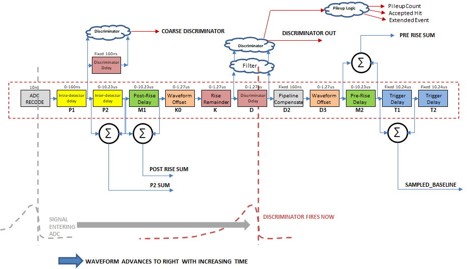
In the middle of the pipeline multiple delay buffers with accumulators provide running sums of the data spanning programmable ranges of time.
Pipeline Structure
The pipeline structure found in every channel is shown as Figure 3. The signal enters at the left and propagates to the right with time, backwards of a traditional oscilloscope image. When the edge of the signal reaches the middle, where the discriminator logic lies, the discriminator fires, capturing all the sum values shown plus timestamp and status information.
- Note the discriminator in the middle of the design across buffer ‘d’, and the coarse discriminator placed well earlier in the pipeline.
The channel pipelines have two basic modes of operation, Leading-Edge Discriminator and Constant-Fraction Discriminator. Data in both modes reads out as a packet consisting of header followed by waveform.
Readout Data Format
VME data readout is always 32-bit words. A header type value in the header indicates which mode the channel was in when the data was taken. A header length field indicates how many 32-bit words are in the header, and a separate packet length field states the total length of header plus waveform.
Data Header
The header format for the ANL digitizer was updated with header types 7 & 8 for the August 2021 release. Header type 7 corresponds to LED mode, and header type 8 corresponds to CFD mode of operation. All data read from the digitizer is 32 bits wide, and the header is 14 words long.
Go Back to Advanced User Guides
Go back to Digital Gammasphere Upgrade Project


